Difference between revisions of "Shinobi (SEGA System 16B)"
From
| Line 80: | Line 80: | ||
== Credits == | == Credits == | ||
*PCB picture from eBay | *171-5521 PCB picture from eBay | ||
*171-5358 PCB picture from Corrado Tomaselli | |||
*Updated schematics from Channelmaniac | *Updated schematics from Channelmaniac | ||
Revision as of 18:44, 9 March 2021
PCB
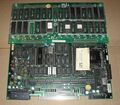
171-5521
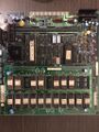
171-5358


PLD's
Motherboard
| PLD Information | Credits | Download | View | |||||
|---|---|---|---|---|---|---|---|---|
| Dump Method | Target Device | Location | ID | Status | Creator(s) | Tester(s) | Files | Pictures |
| Bruteforced | GAL16V8 | 8G | 315-5213 | Tested | Apocalypse | Apocalypse | JEDEC | 
|
| Converted | GAL16V8 | 13F | 315-5214 | Tested | Unknown | Caius | JEDEC | 
|
171-5521 ROM board
| PLD Information | Credits | Download | Pictures | |||||
|---|---|---|---|---|---|---|---|---|
| Dump Method | Target Device | Location | ID | Status | Creator(s) | Tester(s) | Files | View |
| Unlocked
Converted |
PLS153
GAL18V10 |
10B | 315-5298 | Tested | Porchy | Caius | ZIP | 
|
Reference
Credits
- 171-5521 PCB picture from eBay
- 171-5358 PCB picture from Corrado Tomaselli
- Updated schematics from Channelmaniac